Best PCB Design Training in Velachery ⭐ PCB Design Course in Velachery | Updated 2026
Home » Electronic Design Training in Chennai » PCB Design Training in Velachery

PCB Design Training in Velachery

Rated #1 Recoginized as the No.1 Institute for PCB Design Online Course in Chennai

Unlock exciting career prospects with our PCB design online course in Chennai. This specialized course offers hands-on experience and expert guidance to help you master the techniques required to create efficient, reliable, and cost-effective printed circuit boards (PCBs) for a range of industries.

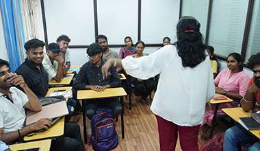
Our PCB Design online training in Chennai covers essential tools and principles such as schematic capture, PCB layout design, signal integrity, thermal management, and manufacturing processes, allowing you to work on real-world projects. By mastering the PCB design training process from concept to production, you will be well-equipped to excel in the electronics field, enhancing your technical expertise and career opportunities.

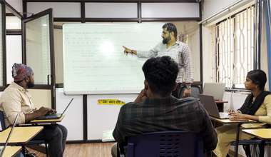
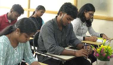
  • Gain practical experience through live projects and real-time case studies.
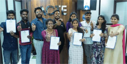
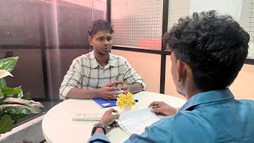
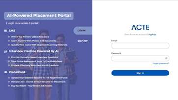
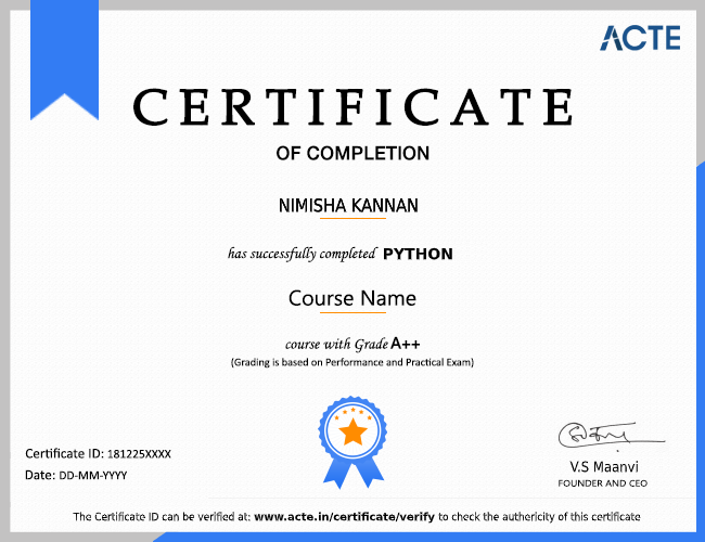
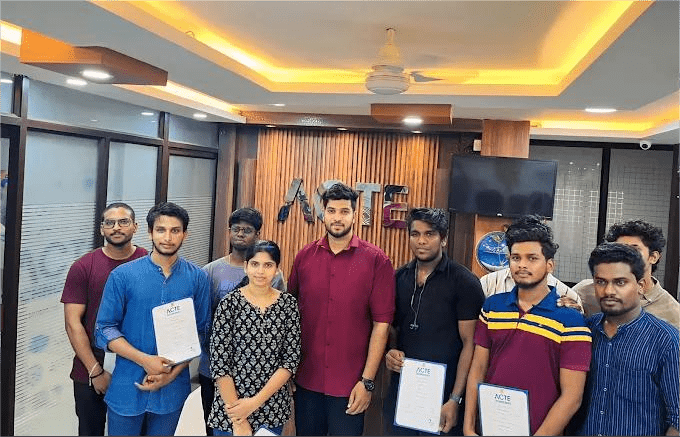
  • Earn your PCB Design certification with placement support and enhance your portfolio.
  • Develop expert skills with our PCB Design course. With over 500+ recruitment partners.
  • Join our PCB Design Online Training today and take the first step toward a thriving career.
  • Our curriculum aligns with industry demands, ensuring you’re prepared for career opportunities.
  • Receive personalized mentoring and career support to guide toward success in the PCB design.
  • Choose Our PCB Design Training Institute In Velachery To Unlock New Opportunities.
  • The PCB Design Course Covers All The Concepts, Tools, And Syllabus For Real-World Expertise.
  • Get Assistance With Career Guidance And Placement Support To Build A Strong Future.
  • Gain Confidence Through Electronic Circuit And PCB Layout Projects Designed For Industry Growth.

Job Assistance

1,200+ Enrolled

In collaboration with

65+ Hrs.

Duration

Online/Offline

Format

LMS

Life Time Access

Quality Training With Affordable Fee

⭐ Fees Starts From

INR 36,000
INR 16,500
100% Placements | Get Hired in Top MNC

Our Hiring Partners

Gain Our Practical PCB Design Training in Velachery

  • Gain practical PCB design chops to produce accurate, dependable electronic circuits. Learn to optimize layouts, manage factors, and insure your boards are manufacturable. Work on real systems to gain hands- on experience and practical knowledge.
  • Make a strong grasp of crucial generalities, like schematic prisoner and element placement. Exercise signal routing, subcaste operation, and design verification. Use these chops to produce error-free boards. Learn marketable and artificial PCB design styles.
  • Master the full PCB design workflow, from tool setup to board mound- up. Optimize layouts and integrate with simulation and testing software. Address real- world problems and deliver professional- quality designs. Figure confidence at every stage of PCB systems.
  • Work on practical scripts, including multi-layer board design, high- speed routing, thermal operation, and prototype testing. Exercise working real challenges and gain experience that prepares you for assistance systems.
  • Train with assistance professionals who partake in practical perceptivity, real- world exemplifications, and guidance. Learn how top contrivers approach systems and avoid common miscalculations. Gain mentorship to make your confidence.
  • Get placement support, including capsule medication, mock interviews, career guidance, and job referrals. Make a strong profile and secure places in electronics, tackle, and PCB design companies and that employers value most.

What You Will Learn in PCB Design Training

Kick-start your journey with PCB design training. Master schematic capture, PCB layout, component placement, and routing.

Develop hands-on skills with real scenarios. Design multi-layer boards, optimize signal integrity, and manage thermal.

Learn how to install and configure PCB design tools, simulate circuits, check design rules, and generate files for production.

Earn a recognized certification and enhance your career through expert training, practical exercises, and placement support.

Your IT Career Starts Here

550+ Students Placed Every Month!

Get inspired by their progress in the Career Growth Report.

Other Categories Placements
  • Non-IT to IT (Career Transition) 2371+
  • Diploma Candidates3001+
  • Non-Engineering Students (Arts & Science)3419+
  • Engineering Students3571+
  • CTC Greater than 5 LPA4542+
  • Academic Percentage Less than 60%5583+
  • Career Break / Gap Students2588+

Upcoming Batches For Classroom and Online

Weekdays
13 - Apr - 2026
08:00 AM & 10:00 AM
Weekdays
15 - Apr - 2026
08:00 AM & 10:00 AM
Weekends
18 - Apr - 2026
(10:00 AM - 01:30 PM)
Weekends
19 - Apr - 2026
(09:00 AM - 02:00 PM)
Can't find a batch you were looking for?
INR 16,500
INR 36,000

OFF Expires in

Who Should Take a PCB Design Certification Course

IT Professionals

Non-IT Career Switchers

Fresh Graduates

Working Professionals

Diploma Holders

Professionals from Other Fields

Salary Hike

Graduates with Less Than 60%

Show More

Job Roles For PCB Design Certification Training

PCB Design Engineer

Hardware Design Engineer

Electronics Design Specialist

Embedded Hardware Engineer

PCB Layout Designer

Electronics Test Engineer

Manufacturing Engineer

Quality Assurance Engineer

Show More

What’s included ?

Convenient learning format

📊 Free Aptitude and Technical Skills Training

  • Learn basic maths and logical thinking to solve problems easily.
  • Understand simple coding and technical concepts step by step.
  • Get ready for exams and interviews with regular practice.
Dedicated career services

🛠️ Hands-On Projects

  • Work on real-time projects to apply what you learn.
  • Build mini apps and tools daily to enhance your coding skills.
  • Gain practical experience just like in real jobs.
Learn from the best

🧠 AI Powered Self Interview Practice Portal

  • Practice interview questions with instant AI feedback.
  • Improve your answers by speaking and reviewing them.
  • Build confidence with real-time mock interview sessions.
Learn from the best

🎯 Interview Preparation For Freshers

  • Practice company-based interview questions.
  • Take online assessment tests to crack interviews
  • Practice confidently with real-world interview and project-based questions.
Learn from the best

🧪 LMS Online Learning Platform

  • Explore expert trainer videos and documents to boost your learning.
  • Study anytime with on-demand videos and detailed documents.
  • Quickly find topics with organized learning materials.

Curriculum

Syllabus of PCB Design Course in Velachery
Module 1: Introduction
  • Overview
  • PCB Design Basics
  • Design Workflow
  • Tools Overview
  • Board Types
  • Installation and Setup
  • User Interface
Module 2: Schematic Design
  • Creating Schematics
  • Component Selection
  • Symbol Libraries
  • Electrical Rules
  • Connections and Nets
  • Schematic Verification
Module 3: PCB Layout
  • Board Dimensions
  • Component Placement
  • Layer Management
  • Routing Techniques
  • Clearance Rules
  • Design Rule Checks
Module 4: Signal and Power Integrity
  • Signal Traces
  • Power Planes
  • Grounding Techniques
  • High-Speed Routing
  • Impedance Control
  • Crosstalk Management
Module 5: Multi-Layer Boards
  • Layer Stack-Up
  • Via Types
  • Thermal Management
  • Routing Strategies
  • Design Verification
Module 6: Simulation and Testing
  • Circuit Simulation
  • Signal Analysis
  • Thermal Analysis
  • EMI/EMC Checks
  • Test Points
Module 7: PCB Fabrication
  • Gerber File Generation
  • Drill Files
  • Assembly Drawings
  • Fabrication Guidelines
  • Component Libraries
  • Design for Manufacturability
Module 8: PCB Assembly
  • Soldering Techniques
  • Pick and Place Setup
  • SMT and Through-Hole
  • Component Orientation
  • Assembly Verification
Module 9: Troubleshooting
  • Design Errors
  • Short Circuits
  • Signal Failures
  • Thermal Issues
  • Rework Techniques
  • Debugging Tools
Module 10: Advanced PCB Design
  • High-Density Layouts
  • Custom Footprints
  • Advanced Routing
  • Automation Scripts
  • Design Optimization
Show More
Show Less

Course Objectives

To learn PCB design, basic electronics knowledge is helpful. Familiarity with circuits, components, and computer-aided design tools is an added advantage.
PCB design training is highly valuable. Companies rely on skilled designers to create accurate boards, reduce errors, and ensure reliable electronics products.
Yes, this beginner-friendly course teaches schematic capture, layout, routing, and board verification step by step. You do not need prior PCB design experience.
  • Designing accurate electronic circuits and boards
  • Managing component placement and signal routing
  • Verifying layouts and preparing boards for manufacturing
  • Simulating and testing circuits for reliability
After completing this course, you can work as a PCB Designer, Electronics Design Engineer, Hardware Developer, or PCB Layout Engineer.
  • PCB design software
  • Design verification tools
  • Simulation and testing software
  • Library and component management tools
  • PCB Designer
  • Electronics Design Engineer
  • Hardware Developer
  • PCB Layout Engineer
  • Hands-on experience with real-world boards
  • Manage projects from schematic to fabrication
  • High demand for skilled designers
  • Practical skills for industry-ready work
PCB design is easy to learn with basic electronics knowledge. Step-by-step guidance and practice projects make learning practical and fast.
  • Simulation and testing
  • Preparing boards for production
  • Schematic creation and layout design
  • Routing, signal integrity, and layer management
Show More

Overview of PCB Design Certification Training

This PCB Design Certification course is a great choice for beginners who want to start a career in electronics and PCB design. The course covers everything from basic to advanced topics like PCB layout, schematic design, and component placement. Students will gain practical knowledge through hands-on exercises and real-time projects. We also provide guidance for PCB design internships to help you gain real industry experience. In addition, the course includes placement preparation program that focuses on resume building, mock interviews, and soft skills training to improve your confidence. By the end of the course, you will be ready to attend interviews and apply for PCB design jobs with the right skills and knowledge.

Additional Info

Key Roles and Responsibilities of PCB Design Profession:

  • PCB Layout Designer : A PCB Layout Designer creates the physical layout of a circuit board based on schematics. They place components correctly and ensure smooth signal flow while reducing interference. They also follow design rules and work closely with engineers to meet project requirements.
  • Schematic Design Engineer : A Schematic Design Engineer creates circuit diagrams that show how components are connected. They choose the right components and check if the design will work properly using simulation tools. They also prepare documents needed for production and testing.
  • Signal Integrity Engineer : A Signal Integrity Engineer makes sure that signals travel properly in high-speed PCB designs. They check for issues like noise and interference and fix them using testing and simulation. They improve design quality by adjusting layout and structure.
  • PCB Design Verification Engineer : A PCB Design Verification Engineer checks whether the PCB design meets all required standards. They use tools like DRC and ERC to find errors and test prototypes to ensure proper performance.
  • PCB Manufacturing Support Engineer : This role focuses on making sure the PCB design can be manufactured without problems. They work with production teams to fix issues and provide clear guidelines to ensure smooth manufacturing.

Important Tools Covered in PCB Design Program:

  • Altium Designer : Altium Designer is a professional tool used to design PCB schematics and layouts. It supports multi-layer designs, 3D views, and error checking before production. It is widely used in the electronics industry.
  • Eagle PCB : Eagle PCB is easy to learn and suitable for beginners. It helps in designing schematics and PCB layouts quickly with built-in component libraries and design tools.
  • KiCad : KiCad is a free and open-source PCB design tool. It supports schematic design, PCB layout, and 3D modeling. It is widely used by students and professionals for learning and projects.
  • OrCAD : OrCAD is an advanced PCB design and simulation tool used in industries. It helps in designing complex circuits and testing them before manufacturing.
  • Proteus : Proteus allows users to design and simulate circuits before building them. It is beginner-friendly and also supports microcontroller-based projects.

Essential Skills You’ll Learn in a PCB Design Certification Course:

  • Schematic Design Skills : You will learn how to create clear and accurate circuit diagrams. This helps in planning the design before building the PCB.
  • PCB Layout and Routing Skills : You will learn how to place components and connect them properly. This ensures the circuit works correctly and avoids errors.
  • Knowledge of Design Rules and Standards : You will understand important design rules that help create safe and reliable PCBs that can be manufactured easily.
  • Simulation and Testing Skills : You will learn how to test circuits using simulation tools before production, which helps reduce errors and save time.
  • Problem-Solving and Critical Thinking : You will develop skills to identify and fix design issues quickly, making your work more efficient and professional.

Future Scope of PCB Design Certification:

  • High-Speed Electronics : There is a growing demand for high-speed PCB design in industries like telecom and computing. Skilled designers will have good career opportunities.
  • IoT Devices : PCB designers are needed to create small and efficient boards for IoT devices used in smart homes and wearable technology.
  • Automotive Electronics : Modern vehicles use many electronic systems, especially in electric and smart cars. This creates strong demand for PCB designers.
  • Consumer Electronics : Devices like smartphones and laptops require advanced PCBs. Designers in this field can work on the latest technologies.
  • Renewable Energy & Robotics : PCB design is important in solar systems, wind energy, and robotics. This field offers long-term and high-growth career opportunities.
Show More
Need customized curriculum?

Gain Hands-on Experience With PCB Design Projects

Advance Your Career with PCB Design Training with Placement Support

  • Our PCB Design Program is designed to develop strong practical skills in schematic creation, PCB layout, component placement, routing, signal integrity, and design rule checks.
  • Learners gain hands-on experience with industry-standard PCB design tools, including Altium Designer, Eagle, KiCad, OrCAD, and simulation utilities for signal and power integrity analysis.
  • Our PCB Design Training with Placement Support helps learners explore opportunities in electronics manufacturing companies, PCB fabrication units, embedded system firms, hardware design teams.
  • The Career Support Program provides guidance from experienced PCB designers, helping learners refine schematic entry, layout optimization, component selection, trace routing.
  • Personalized mentoring ensures the knowledge acquired aligns with opportunities in PCB design, hardware engineering, embedded systems, electronics R&D, and product prototyping roles.
  • Completing the course strengthens practical portfolios by highlighting expertise in multi-layer PCB design, high-speed design considerations, DFM compliance, simulation, and layout troubleshooting.
  • Interactive exercises and expert coaching allow learners to apply PCB design principles, create optimized layouts, perform signal simulations, and validate designs for real-world projects for PCB Design Training with Placement Support.

Enhance Your Career with PCB Design Certification

Discover the world of PCB design with a comprehensive course tailored for beginners and electronics professionals. The program delivers hands-on training in schematic development, PCB layout, component placement, routing, signal integrity, DFM checks, and simulation. Learners work with real-world PCB design tools to build practical skills and confidence. Earning this PCB Design Certification can pave the way to roles such as PCB Designer, Hardware Engineer, Embedded System Developer, Electronics Design Engineer, or Product Development Specialist.

Complete Your Course

a downloadable Certificate in PDF format, immediately available to you when you complete your Course

Get Certified

a physical version of your officially branded and security-marked Certificate.

Get Certified

About Our Expert PCB Design Trainers

  • Our PCB Design Trainers guide learners through practical, real-world PCB design tasks, providing hands-on support for schematic creation, PCB layout, routing, and component placement.
  • We leverage strong industry connections to help learners discover opportunities as PCB Designers, Hardware Engineers, Embedded System Developers, and Electronics Design Specialists.
  • Our Trainers are skilled professionals with in-depth experience in PCB design tools and techniques, including Altium Designer, Eagle, KiCad, OrCAD, Gerber generation, and signal integrity analysis.
  • They share practical knowledge gained from working on real-world electronics projects, product development, and PCB manufacturing processes, covering tasks like multi-layer design, DFM checks.
  • The program blends self-paced learning, live interactive sessions, personalized mentoring, and hands-on labs using industry-standard PCB tools to simulate professional PCB design workflows.
  • From basic schematic drafting and component placement to advanced routing, design rule checks, signal integrity, and PCB fabrication preparation, this course equips learners with essential practical skills.

Authorized Partners

ACTE TRAINING INSTITUTE PVT LTD is the unique Authorised Oracle Partner, Authorised Microsoft Partner, Authorised Pearson Vue Exam Center, Authorised PSI Exam Center, Authorised Partner Of AWS .

100% Placements | Get Hired in Top MNC

    Career Support

    Placement Assistance

    Exclusive access to ACTE Job portal

    Mock Interview Preparation

    1 on 1 Career Mentoring Sessions

    Career Oriented Sessions

    Resume & LinkedIn Profile Building

    We Offer High-Quality Training at The Lowest Prices.

    Affordable, Quality Training for Freshers to Launch IT Careers & Land Top Placements.

    What Makes ACTE Training Different?

    Feature

    ACTE Technologies

    Other Institutes

    Affordable Fees

    Competitive Pricing With Flexible Payment Options.

    Higher Fees With Limited Payment Options.

    Industry Experts

    Well Experienced Trainer From a Relevant Field With Practical Training

    Theoretical Class With Limited Practical

    Updated Syllabus

    Updated and Industry-relevant Course Curriculum With Hands-on Learning.

    Outdated Curriculum With Limited Practical Training.

    Hands-on projects

    Real-world Projects With Live Case Studies and Collaboration With Companies.

    Basic Projects With Limited Real-world Application.

    Certification

    Industry-recognized Certifications With Global Validity.

    Basic Certifications With Limited Recognition.

    Placement Support

    Strong Placement Support With Tie-ups With Top Companies and Mock Interviews.

    Basic Placement Support

    Industry Partnerships

    Strong Ties With Top Tech Companies for Internships and Placements

    No Partnerships, Limited Opportunities

    Batch Size

    Small Batch Sizes for Personalized Attention.

    Large Batch Sizes With Limited Individual Focus.

    LMS Features

    Lifetime Access Course video Materials in LMS, Online Interview Practice, upload resumes in Placement Portal.

    No LMS Features or Perks.

    Training Support

    Dedicated Mentors, 24/7 Doubt Resolution, and Personalized Guidance.

    Limited Mentor Support and No After-hours Assistance.

    PCB Design Course FAQs

    Looking for better Discount Price?

    Call now: +91-7669 100 251 and know the exciting offers available for you!
    • ACTE is the Legend in offering placement to the students. Please visit our Placed Students List on our website
    • We have strong relationship with over 700+ Top MNCs like SAP, Oracle, Amazon, HCL, Wipro, Dell, Accenture, Google, CTS, TCS, IBM etc.
    • More than 3500+ students placed in last year in India & Globally
    • ACTE conducts development sessions including mock interviews, presentation skills to prepare students to face a challenging interview situation with ease.
    • 85% percent placement record
    • Our Placement Cell support you till you get placed in better MNC
    • Please Visit Your Student Portal | Here FREE Lifetime Online Student Portal help you to access the Job Openings, Study Materials, Videos, Recorded Section & Top MNC interview Questions
    • Certification is recognized by major global companies, enhancing your career credibility.
    • ACTE is an authorized partner of leading organizations including Oracle, Microsoft, and
    • The course completion certificate validates your practical skills and industry knowledge.
    • Globally accepted certification helps improve job opportunities and professional growth.

    Does the course provide practice tests?

    Yes, practice tests are included. They help you evaluate understanding of schematic design, PCB layout, routing, and board verification. This ensures readiness for real-world projects.

    Who are the course instructors, and how are they selected?

    All instructors are industry professionals with 8–12 years of experience in PCB design, electronics, and hardware development. They are selected based on project experience, domain knowledge, and teaching skills.

    Does the course provide placement assistance?

    Yes, we have partnerships with electronics and hardware companies. Students receive placement support, resume guidance, and interview preparation to secure relevant job roles.

    Is job assistance available after completing the course?

    Yes, support includes hands-on projects, resume building, mock interviews, and technical assessments to help you enter the PCB design industry confidently.

    Why should I enroll in the PCB Design Master Program?

    The program provides hands-on experience in schematic capture, PCB layout, routing, multi-layer boards, and testing. You gain real-world exposure and earn certification recognized by industry employers.

    Is the PCB Design certification valuable?

    Yes, certification validates your skills in PCB design and electronics layout. It enhances your resume and improves your chances for roles like PCB Designer or Electronics Engineer.
    Our courseware is designed to give a hands-on approach to the students in PCB Design. The course is made up of theoretical classes that teach the basics of each module followed by high-intensity practical sessions reflecting the current challenges and needs of the industry that will demand the students’ time and commitment.

    Will I work on live projects?

    Yes, you will complete projects such as schematic design, PCB layout, multi-layer routing, and prototype testing. These build practical skills for industry readiness.

    What if I miss one or more classes?

    You can access recorded sessions, request backup lessons, and use provided study materials to catch up.

    Which training modes are available?

    Flexible options include classroom training, online live sessions, one-on-one mentoring, fast-track batches, and corporate training programs.

    Why should I choose this PCB Design Course in Velachery?

    The course offers industry-focused curriculum, expert trainers, hands-on projects, certification, and placement support to make you job-ready.

    Will I receive adequate hands-on training?

    Yes, the course includes real-time projects, practical exercises, and PCB design simulations to ensure strong hands-on experience.
    You can contact our support number at +91 76691 00251 Directly can do by ACTE.in's E-commerce payment system Login or directly walk-in to one of the ACTE branches in India
    Show More

    Job Opportunities in PCB Design

    More Than 35% of Individuals Prefer PCB Design. PCB Design is One of the Most Popular and in-demand Technology in the Designing World.