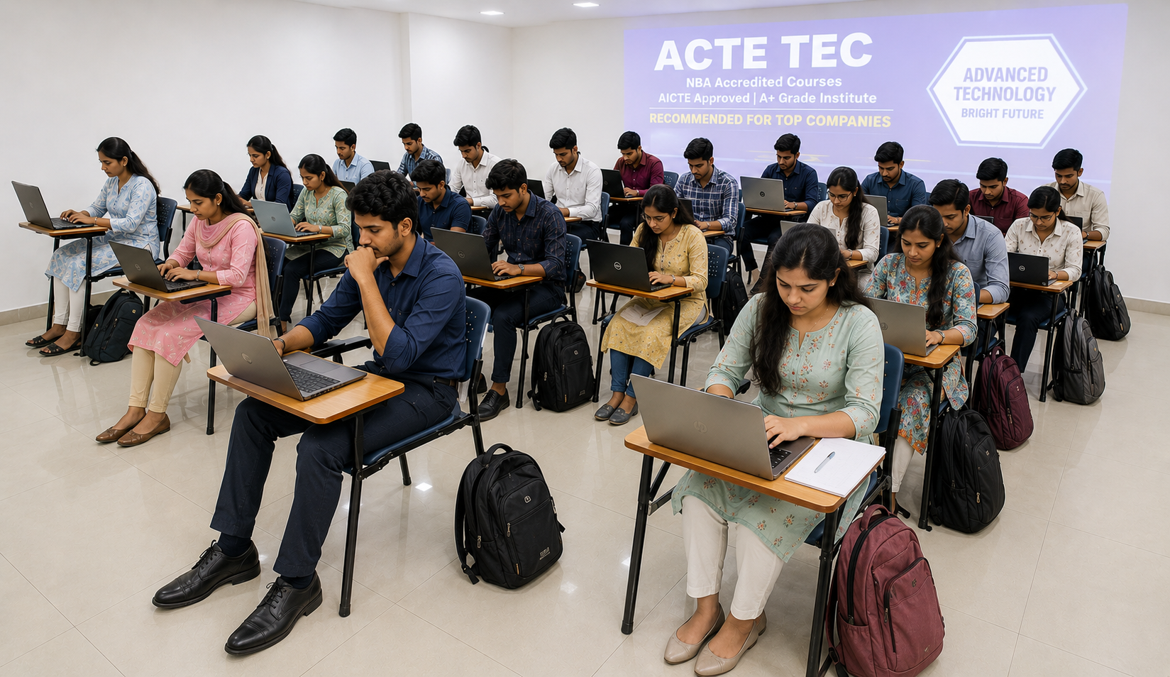
Rated #1 Recoginized as the No.1 Institute for PCB Designing Course in Coimbatore
Our PCB Designing Course in Coimbatore offers a comprehensive, hands-on learning experience for professionals eager to earn their PCB design certification and master the art of designing printed circuit boards.
This course covers essential topics such as PCB layout design, schematic capture, signal integrity, PCB manufacturing processes, and the use of industry-standard software like Eagle and Altium. Gain the skills and knowledge needed to design efficient, reliable, and cost-effective PCBs for various electronic applications.
- Enroll now to enhance your PCB design skills!
- Stay ahead in electronics design with expert-led mentorship.
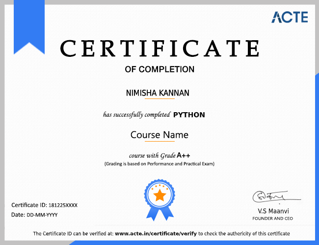
- Become a certified PCB design expert and fast-track your career.
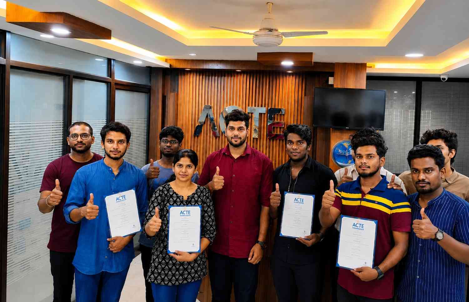
- Join 350+ companies and 13,898+ graduates mastering PCB design.
- Learn PCB designing with an affordable, industry-recognized curriculum.
- Unlock global career opportunities in the dynamic electronics and embedded systems industries.