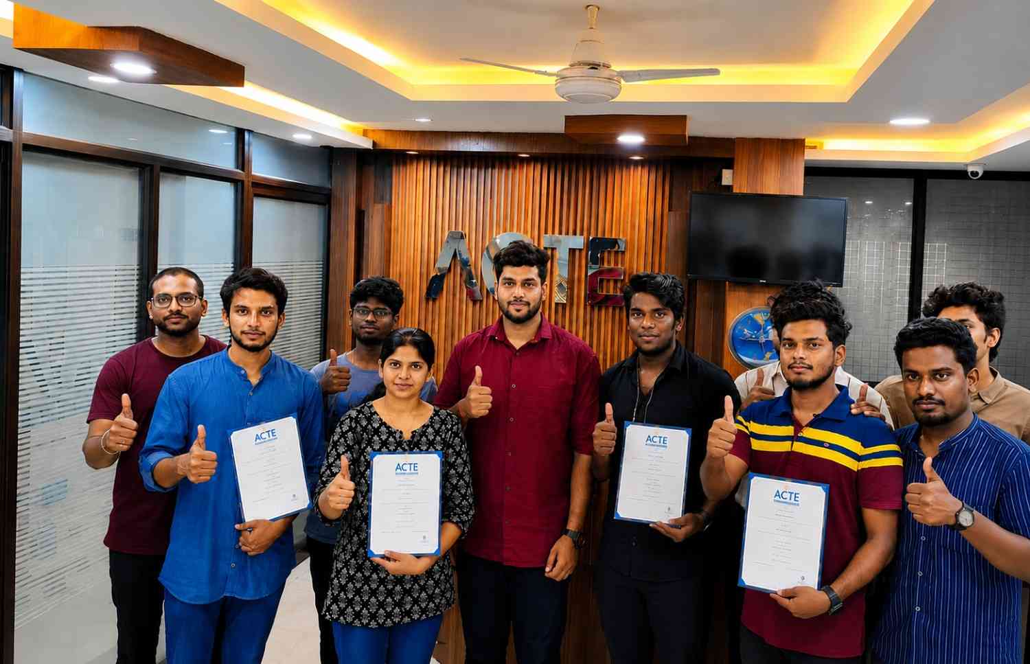
Complete PCB Design Course in Mumbai for Industry Skills
PCB Design Course in Mumbai offers comprehensive learning on the complete PCB development process, covering circuit basics, schematic preparation, component selection, PCB architecture, layout design, routing, testing, and manufacturing. The program introduces learners to professional design methods such as component positioning, layer configuration, power management, signal integrity, design rule verification, multilayer PCB development, and fabrication documentation. Through practical assignments, live projects, and hands-on activities, participants gain experience with industry-relevant PCB design software and workflows. The PCB Design Course in Mumbai training also covers troubleshooting, design enhancement, prototype development, testing methods, and production requirements. Learners develop the technical capabilities required to design dependable and efficient circuit boards for embedded systems, IoT products, automotive electronics, consumer devices, automation solutions, and industrial applications. The program is suitable for students, graduates, electronics professionals, and aspiring PCB designers seeking practical industry-focused expertise and career opportunities in hardware and electronics development.
Additional Information
Career Roles After PCB Design Training Institute in Mumbai
- PCB Design Engineer: Creates detailed PCB layouts, manages board specifications, and ensures designs follow electrical, mechanical, and manufacturing requirements.
- Hardware Design Engineer: Develops hardware solutions, integrates electronic components, and works with PCB teams to build dependable and functional systems.
- PCB Testing Engineer: Performs PCB design verification, testing, and debugging to identify design problems, improve performance, and ensure dependable operation before production.
- Embedded Hardware Engineer: Designs embedded hardware by integrating PCB layouts with microcontrollers, sensors, and electronic components for different applications.
- PCB Manufacturing Engineer: Supports PCB fabrication by reviewing production files, addressing manufacturing concerns, coordinating assembly operations, and maintaining quality standards.
- Electronic Product Engineer: Oversees electronic product development by coordinating design, testing, revisions, troubleshooting, and improvements throughout the product lifecycle.
Software Tools and Technologies Covered in PCB Design Certification Course in Mumbai
- Mentor Graphics PADS: Helps designers create schematics, develop PCB layouts, perform design verification, and prepare manufacturing-ready boards for production.
- CircuitMaker: Enables collaborative PCB development by allowing learners to create schematics, organize component libraries, and build effective layouts for electronic projects.
- LTspice: Offers circuit simulation for evaluating electrical behavior, verifying performance, identifying design problems, and enhancing electronic system reliability.
- MATLAB Simulink: Enables system modeling and simulation to evaluate electronic designs, study performance, and understand embedded system applications efficiently.
- Gerber File Generation Tools: Produce precise manufacturing files that enable effective communication between PCB designers and fabrication teams throughout board production.
- 3D PCB Visualization Tools: Enable designers to inspect board structures, verify component positioning, assess mechanical compatibility, and preview PCB layouts before manufacturing.
Career Opportunities After PCB Design Placement Training in Mumbai
- PCB Application Engineer: Supports PCB development, offers technical assistance, enhances designs, and ensures circuit boards satisfy application and performance requirements.
- Design Verification Engineer: Evaluates PCB designs, verifies functionality, detects issues, and ensures electronic systems satisfy expected performance and reliability standards.
- Hardware Development Engineer: Designs and integrates electronic hardware, collaborates with PCB teams, and improves product performance across various applications.
- Electronics Testing Engineer: Conducts circuit testing, detects hardware faults, resolves technical problems, and improves the reliability and performance of electronic products.
- Technical Design Consultant: Offers PCB design expertise, suggests improvements, advises engineering teams, and supports the creation of effective electronic solutions.
- Electronic Manufacturing Engineer: Oversees PCB production and assembly processes, addresses manufacturing challenges, and maintains quality standards for electronic products.
Future Opportunities for PCB Design Internship Training in Mumbai
- Growth of Smart Electronics: Increasing adoption of smart devices, connected systems, and automation technologies is creating greater demand for skilled PCB design professionals.
- Expansion of IoT Product Development: IoT products require compact, efficient, and dependable circuit boards, creating opportunities for trained PCB design professionals.
- Progress in Automotive Electronics: Modern vehicles depend on sophisticated electronic systems and control units, increasing demand for professionals with PCB design expertise.
- Rising Medical Electronics: Healthcare equipment requires dependable electronic circuits and PCB solutions, creating opportunities in medical device design and development.
- Innovation in Semiconductor Applications: Developments in electronic components, chip technologies, and compact devices are increasing demand for professionals skilled in PCB development.
- Global Career Opportunities: PCB design expertise can create international career possibilities with electronics manufacturers, technology firms, and organizations developing advanced products.
Show More

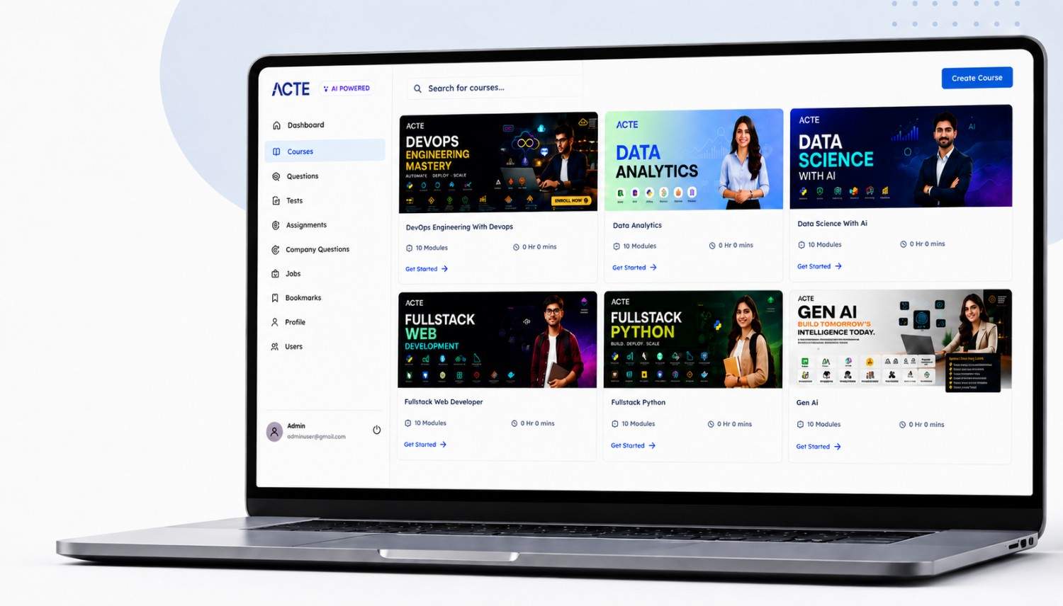
 LMS
LMS