
Best PCB Design Training in Porur ⭐ PCB Design Certification Course in Porur | Updated 2026
Home » Electronic Design Training in Chennai » PCB Design Training in Porur

PCB Design Training in Porur

Rated #1 Recoginized as the No.1 Institute for PCB Design Online Course in Chennai

Unlock exciting career prospects with our PCB design online course in Chennai. This specialized course offers hands-on experience and expert guidance to help you master the techniques required to create efficient, reliable, and cost-effective printed circuit boards (PCBs) for a range of industries.

Our PCB Design online training in Chennai covers essential tools and principles such as schematic capture, PCB layout design, signal integrity, thermal management, and manufacturing processes, allowing you to work on real-world projects. By mastering the PCB design training process from concept to production, you will be well-equipped to excel in the electronics field, enhancing your technical expertise and career opportunities.

  • Gain practical experience through live projects and real-time case studies.
  • Earn your PCB Design certification with placement support and enhance your portfolio.
  • Develop expert skills with our PCB Design course. With over 500+ recruitment partners.
  • Join our PCB Design Online Training today and take the first step toward a thriving career.
  • Our curriculum aligns with industry demands, ensuring you’re prepared for career opportunities.
  • Receive personalized mentoring and career support to guide toward success in the PCB design.
  • Grow With PCB Design Training Institute in Porur As The Best Choice For Your Future.
  • Boost Your Career By This Course With Complete Placement Support and Interview Guidance.
  • Choose the Learning Path That Aligns With Your Lifestyle, Weekday, Weekend, and Fast-Track Formats.
  • Advance With Projects And Practical Learning Modes That Match Your Professional Goals.

Job Assistance

1,200+ Enrolled

In collaboration with

65+ Hrs.

Duration

Online/Offline

Format

LMS

Life Time Access

Quality Training With Affordable Fee

⭐ Fees Starts From

INR 36,000
INR 16,500
100% Placements | Get Hired in Top MNC

Our Hiring Partners

Gain Our Practical PCB Design Training in Porur

  • Enroll in PCB Design training in Porur to build practical skills in printed circuit board design through expert-led sessions, hands-on projects, and industry-focused learning. Ideal for students, engineers, and professionals aiming to excel in the electronics design industry.
  • Learn the complete PCB design workflow, starting with electronic fundamentals, schematic creation, and component selection before advancing to industry-standard tools like KiCad and Altium Designer. The structured curriculum ensures strong technical knowledge and practical expertise.
  • Gain valuable hands-on experience by working on live PCB projects involving circuit simulation, PCB layout, component placement, routing techniques, and design rule verification. Practical training helps you understand manufacturing standards and real-world design challenges.
  • Enhance your expertise with advanced topics including multilayer PCB design, signal integrity analysis, EMI/EMC compliance, high-speed PCB layout, and embedded system integration. These modules prepare you to handle complex electronic product development with confidence.
  • Our PCB Design training in Porur also includes career-focused support such as resume building, interview preparation, technical guidance, and placement assistance. Meet the growing demand for skilled PCB designers across electronics, automotive, IoT, and embedded industries.
  • Build a rewarding career in electronics by joining our PCB Design Training in Porur. Develop industry-relevant skills, gain practical project experience, and learn from experienced trainers to confidently pursue opportunities in PCB design, product development, and manufacturing.

What You Will Learn in PCB Design Training Course

Master industry-leading PCB design tools such as Eagle and Altium Designer while learning schematic capture and layout optimization through practical, hands-on training.

Explore advanced PCB design concepts including multilayer board design and high-speed PCB layout techniques used in modern electronic products.

Learn to install and configure PCB design software, perform design rule checks (DRC), and generate manufacturing-ready files for accurate PCB fabrication and assembly.

Build a strong foundation in electronics and circuit design by understanding schematic diagrams and how they interact to create efficient and reliable PCB designs.

Your IT Career Starts Here

550+ Students Placed Every Month!

Get inspired by their progress in the Career Growth Report.

Other Categories Placements
  • Non-IT to IT (Career Transition) 2371+
  • Diploma Candidates3001+
  • Non-Engineering Students (Arts & Science)3419+
  • Engineering Students3571+
  • CTC Greater than 5 LPA4542+
  • Academic Percentage Less than 60%5583+
  • Career Break / Gap Students2588+

Upcoming Batches For Classroom and Online

Weekdays
10 - August - 2026
08:00 AM & 10:00 AM
Weekdays
12 - August - 2026
08:00 AM & 10:00 AM
Weekends
15 - August - 2026
(10:00 AM - 01:30 PM)
Weekends
16 - August - 2026
(09:00 AM - 02:00 PM)
Can't find a batch you were looking for?
INR 16,500
INR 36,000

OFF Expires in

Who Should Take a PCB Design Certification Course

IT Professionals

Non-IT Career Switchers

Fresh Graduates

Working Professionals

Diploma Holders

Professionals from Other Fields

Salary Hike

Graduates with Less Than 60%

Show More

Job Roles For PCB Design Certification Training

PCB Design Engineer

Hardware Design Engineer

Electronics Design Specialist

Embedded Hardware Engineer

PCB Layout Designer

Electronics Test Engineer

Manufacturing Engineer

Quality Assurance Engineer

Show More

What’s included ?

Convenient learning format

📊 Free Aptitude and Technical Skills Training

  • Learn basic maths and logical thinking to solve problems easily.
  • Understand simple coding and technical concepts step by step.
  • Get ready for exams and interviews with regular practice.
Dedicated career services

🛠️ Hands-On Projects

  • Work on real-time projects to apply what you learn.
  • Build mini apps and tools daily to enhance your coding skills.
  • Gain practical experience just like in real jobs.
Learn from the best

🧠 Launch Your Career in Top MNC Companies

  • Master technical and HR interview rounds.
  • Gain confidence with expert mock interview practice.
  • Improve your chances of getting hired faster.
Learn from the best

🎯 Interview Preparation For Freshers

  • Practice company-based interview questions.
  • Take online assessment tests to crack interviews
  • Practice confidently with real-world interview and project-based questions.
Learn from the best

🧪 LMS Self Learning Platform

  • Explore expert trainer videos and documents to boost your learning.
  • Study anytime with on-demand videos and detailed documents.
  • Top MNC interview questions & self coding practice.

Curriculum

Syllabus of PCB Design Training in Porur
Module 1: Fundamentals of Electronics and PCBs
  • Overview of electronic components
  • Standards and symbols for circuits
  • PCB types
  • Overview of PCB fabrication
  • Fundamentals of design flow
  • Applications in industry
Module 2:Design Schematics
  • Fundamentals of schematic capture
  • Selection of components
  • Techniques for net labelling
  • Hierarchy of design
  • Checks for electrical rules (ERC)
Module 3: Foundations of PCB Layout
  • construction of a board outline
  • Layer stack-up fundamentals
  • Rules for component placement
  • Fundamentals of routing
  • Clearance Rules
  • Design Rule Checks
Module 4: PCB Design in Single and Double Layers
  • Design of a single-layer board
  • Routing techniques using two layers
  • Through usage and types
  • Component placement strategies for optimised layout
  • Component placement strategies for optimised layoutl
  • Crosstalk Management
Module 5: Design of Multilayer PCBs
  • Layer Stack-Up
  • Via Types
  • Planning for multilayer stacks
  • Fundamentals of signal integrity
  • High-speed route ideas
  • EMI/EMC factors
  • Thermal control
Module 6: Tools for PCB Design
  • Overview of PCB instruments
  • creation of libraries
  • Management of footprints
  • Setup of design rules
  • Test Points
Module 7: Fabrication & Manufacturing
  • Generation of Gerber files
  • Pick-and-place and drill files
  • PCB manufacturing procedure
  • Methods of assembly
  • Typical manufacturing problems
  • Design for Manufacturability
Module 8: Debugging and Testing
  • Soldering Techniques
  • Testing for functionality
  • Debugging methods
  • Rework procedures
  • Assembly Verification
Module 9: Industry Practices & Real-Time Projects
  • Standards for industry design
  • Project work depending on clients
  • Design documentation
  • Version control and collaboration workflows
  • Testing, validation, and prototype review processes
  • Debugging Tools
Module 10: Advanced PCB Design
  • High-Density Layouts
  • Custom Footprints
  • Advanced Routing
  • Automation Scripts
  • Design Optimization
Show More
Show Less

Course Objectives

A basic understanding of electronics and electrical circuits is beneficial for learning PCB design. Familiarity with electronic components and CAD software can help you learn more effectively, but beginners can also enroll.

Yes. PCB design skills are highly valued across industries such as electronics, automotive, telecommunications, and embedded systems. This training can improve your career prospects and open opportunities in hardware design.

Absolutely. The course starts with the basics of electronics and gradually covers schematic design, PCB layout, routing, and board validation, making it suitable for learners without prior experience.
  • Develop professional PCB layouts from electronic schematics
  • Learn efficient component placement and signal routing techniques
  • Validate PCB designs before manufacturing
  • Perform circuit simulation and design verification
Upon successful completion of the course, you can pursue roles such as PCB Designer, PCB Layout Engineer, Electronics Design Engineer, Hardware Engineer, or Embedded Hardware Developer.
  • PCB design and layout software
  • Design verification and validation tools
  • Circuit simulation software
  • Component library management tools
  • PCB Designer
  • PCB Layout Engineer
  • Electronics Design Engineer
  • Hardware Engineer
  • Gain practical experience through real-time projects
  • Learn the complete PCB development lifecycle
  • Build industry-relevant technical skills
  • Increase employability in the electronics sector
PCB design is easy to learn with the right guidance. This course provides step-by-step instruction, practical exercises, and real-world projects to help learners build confidence and technical expertise.
  • PCB Design Engineer
  • PCB Layout Designer
  • Electronics Design Engineer
  • Hardware Engineer
Yes. Beginners can successfully learn PCB design through structured training that covers electronics fundamentals, schematic capture, PCB layout, routing, and design validation. Regular hands-on practice helps develop professional-level skills.
Yes. As industries continue to adopt advanced electronics, IoT, automation, and embedded technologies, the demand for skilled PCB designers continues to grow. Completing this course equips you with practical skills, strong career opportunities, and long-term professional growth.
Show More

Overview Of PCB Design Course In Porur

Kickstart your career in the electronics industry with our PCB Design course in Porur thoughtfully designed for students, fresh graduates, diploma holders, engineering professionals, and beginners who want to develop practical PCB design skills. The curriculum begins with the fundamentals of electronics and gradually progresses to advanced concepts, including schematic capture, PCB layout design, component placement, signal routing, multilayer board design, design rule checking (DRC), circuit verification, and manufacturing file generation. Through real-time projects and industry-oriented assignments, learners gain valuable hands-on experience using professional PCB design tools widely adopted in the electronics industry. Our PCB Design placement course in Porur emphasizes practical learning through lab sessions, live project implementation, and case studies that help students understand real-world PCB development workflows. In addition to technical training, we provide internship assistance, placement support, resume preparation, aptitude training, mock interviews, and communication skill development to enhance employability. Experienced trainers offer personalized guidance to ensure every learner gains confidence in designing reliable and efficient printed circuit boards.

Additional Info

Job Roles and Responsibilities for PCB Design Professional

  • PCB Design Engineer: Designs high-quality printed circuit boards by creating schematics, placing components, routing signals, performing design verification, and preparing manufacturing-ready PCB files.
  • PCB Layout Designer: Transforms electronic schematics into optimized PCB layouts by managing layer stack-ups, trace routing, component placement, and ensuring compliance with design rules.
  • Hardware Engineer: Develops electronic hardware by integrating PCB designs with processors, sensors, power circuits, and peripherals while testing performance, reliability, and functionality.
  • Electronics Design Engineer: Designs, analyzes, and validates electronic circuits using PCB design tools to ensure products meet quality, safety, efficiency, and industry performance requirements.
  • Electronics R&D Engineer: Researches innovative electronic solutions, develops advanced PCB prototypes, evaluates new technologies, and improves circuit designs for future electronic products and applications.
  • Manufacturing Support Engineer: Supports PCB production by reviewing fabrication files, resolving manufacturing issues, optimizing assembly processes, and ensuring consistent product quality.

Important Tools Covered in PCB Design Placement Training in Porur

  • Altium Designer: Learn industry-standard PCB design using Altium Designer for schematic capture, PCB layout, signal routing, design validation, and manufacturing file generation.
  • KiCad: Master KiCad to create professional schematics, PCB layouts, and multilayer board designs using its powerful open-source design and verification features.
  • Autodesk Eagle CAD: Explore Autodesk Eagle CAD to design schematics, develop PCB layouts, manage component libraries, and accelerate prototype development with cloud support.
  • Proteus Design Suite: Use Proteus to simulate electronic circuits, test embedded systems, validate microcontroller applications, and design reliable PCBs before fabrication.
  • EasyEDA: Gain hands-on experience with EasyEDA for browser-based schematic design, PCB layout creation, component management, and rapid prototype development.
  • Cadence OrCAD: Learn Cadence OrCAD to develop complex PCB designs, perform circuit simulation, verify layouts, and generate production-ready files for industrial applications.

Essential Skills You’ll Learn in a PCB Design Certification Course in Porur:

  • PCB Design Engineering: Learn to create professional PCB layouts, optimize component placement, perform signal routing, and generate manufacturing-ready designs for electronic products.
  • Hardware Design: Develop the skills to design, integrate, and test electronic hardware by combining PCB layouts with components to build reliable and efficient systems.
  • Electronics Circuit Design: Gain expertise in designing, analyzing, and validating electronic circuits while ensuring PCB designs meet industry standards for performance and reliability.
  • Research and Development: Build the ability to develop innovative PCB prototypes, evaluate circuit performance, troubleshoot issues, and support next-generation electronic product development.
  • Product Development: Master PCB design techniques required to develop high-quality electronic products by focusing on functionality, manufacturability, testing, and product reliability.
  • Manufacturing and Testing: Learn to verify PCB designs, perform testing, identify design issues, prepare fabrication files, and ensure smooth manufacturing with consistent product quality.

Future Scope of PCB Design Course Institute in Porur:

  • Growing Electronics Industry: PCB design professionals are in high demand as consumer electronics, industrial automation, medical devices, and smart technologies continue to expand globally.
  • IoT and Embedded Systems: Build a career in IoT and embedded systems by designing compact, high-performance PCBs that power smart devices, sensors, and connected technologies.
  • Automotive and Electric Vehicles: Advance your career in automotive electronics by designing reliable PCBs for electric vehicles, ADAS, battery management systems, and autonomous technologies.
  • Aerospace and Defence: PCB designers are needed to develop high-reliability circuit boards for aerospace, defence, satellite, and mission-critical electronic systems with strict standards.
  • Research and Product Innovation: Gain opportunities in R&D by developing advanced PCB solutions, improving electronic products, and contributing to innovative hardware technologies.
  • Global Career Opportunities: PCB design certification opens doors to international careers in electronics manufacturing, hardware development, embedded systems, and product engineering.
Show More
Need customized curriculum?

Gain Hands-on Experience With PCB Design Projects

Our Best Hiring Partners for PCB Design Placement

  • Our PCB Design placement program connects students with leading electronics and engineering companies, creating excellent career opportunities in hardware and embedded technology.
  • We partner with renowned companies such as Accenture, TCS, Wipro, IBM, Cognizant, and Infosys, along with technology firms offering diverse engineering and technical roles.
  • Students gain placement opportunities with startups and established companies in electronics, IoT, automation, and PCB design, where practical expertise is highly valued.
  • Our placement training includes aptitude preparation, technical mock interviews, HR sessions, resume building, and communication skills to improve interview performance.
  • Hiring companies value candidates with hands-on PCB project experience, as it reflects practical knowledge, design expertise, troubleshooting skills, and industry readiness.
  • Students receive expert guidance to create professional project portfolios that effectively highlight their PCB design knowledge, technical abilities, and real-world achievements.
  • Growing demand across electronics industries creates excellent career prospects, and our PCB Design placement support helps students secure rewarding engineering opportunities.

Enhance Your Career with PCB Design Certification

Advance your electronics career with our industry-focused PCB Design Certification, suitable for beginners and working professionals. Gain hands-on experience in schematic capture, PCB layout design, component placement, signal integrity analysis, Design for Manufacturing verification, and circuit simulation using industry-standard software. Build practical expertise through real-time projects and prepare for rewarding roles such as PCB Designer, Hardware Engineer, Electronics Design Engineer, and Product Development Engineer.

Complete Your Course

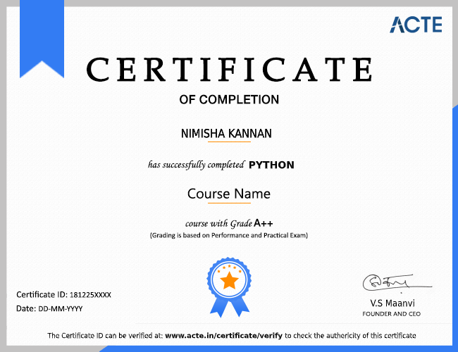
a downloadable Certificate in PDF format, immediately available to you when you complete your Course

Get Certified

a physical version of your officially branded and security-marked Certificate.

Get Certified

About Our Expert PCB Design Trainers in Porur

  • Learn from experienced PCB Design trainers in Porur who deliver practical, industry-focused training, simplifying complex concepts and building strong PCB design fundamentals.
  • Our trainers provide hands-on guidance with Proteus, KiCad, and Altium Designer, enabling students to design, simulate, and develop professional PCB projects confidently.
  • Receive personalized mentoring in schematic creation, PCB layout design, routing techniques, and troubleshooting, ensuring every student gains practical skills with confidence.
  • Our certified PCB Design trainers have 7+ years of industry experience, real-time project expertise, and offer career-focused guidance with placement support from MNC professionals.
  • Training includes PCB industry standards, documentation practices, manufacturing guidelines, and testing techniques to prepare students for successful electronics and hardware careers.
  • With expert guidance, students develop strong technical knowledge, practical project experience, problem-solving abilities, and the confidence to excel in PCB Design careers.

Authorized Partners

ACTE TRAINING INSTITUTE PVT LTD is the unique Authorised Oracle Partner, Authorised Microsoft Partner, Authorised Pearson Vue Exam Center, Authorised PSI Exam Center, Authorised Partner Of AWS .

100% Placements | Get Hired in Top MNC

    Career Support

    Placement Assistance

    Exclusive access to ACTE Job portal

    Mock Interview Preparation

    1 on 1 Career Mentoring Sessions

    Career Oriented Sessions

    Resume & LinkedIn Profile Building

    We Offer High-Quality Training at The Lowest Prices.

    Affordable, Quality Training for Freshers to Launch IT Careers & Land Top Placements.

    What Makes ACTE Training Different?

    Feature

    ACTE Technologies

    Other Institutes

    Affordable Fees

    Competitive Pricing With Flexible Payment Options.

    Higher Fees With Limited Payment Options.

    Industry Experts

    Well Experienced Trainer From a Relevant Field With Practical Training

    Theoretical Class With Limited Practical

    Updated Syllabus

    Updated and Industry-relevant Course Curriculum With Hands-on Learning.

    Outdated Curriculum With Limited Practical Training.

    Hands-on projects

    Real-world Projects With Live Case Studies and Collaboration With Companies.

    Basic Projects With Limited Real-world Application.

    Certification

    Industry-recognized Certifications With Global Validity.

    Basic Certifications With Limited Recognition.

    Placement Support

    Strong Placement Support With Tie-ups With Top Companies and Mock Interviews.

    Basic Placement Support

    Industry Partnerships

    Strong Ties With Top Tech Companies for Internships and Placements

    No Partnerships, Limited Opportunities

    Batch Size

    Small Batch Sizes for Personalized Attention.

    Large Batch Sizes With Limited Individual Focus.

    LMS Features

    Lifetime Access Course video Materials in LMS, Online Interview Practice, upload resumes in Placement Portal.

    No LMS Features or Perks.

    Training Support

    Dedicated Mentors, 24/7 Doubt Resolution, and Personalized Guidance.

    Limited Mentor Support and No After-hours Assistance.

    PCB Design Training FAQs

    Looking for better discount price?

    Call now: +91-7669 100 251 and know the exciting offers available for you!
    • ACTE is the Legend in offering placement to the students. Please visit our Placed Students List on our website
    • We have strong relationship with over 700+ Top MNCs like SAP, Oracle, Amazon, HCL, Wipro, Dell, Accenture, Google, CTS, TCS, IBM etc.
    • More than 3500+ students placed in last year in India & Globally
    • ACTE conducts development sessions including mock interviews, presentation skills to prepare students to face a challenging interview situation with ease.
    • 85% percent placement record
    • Our Placement Cell support you till you get placed in better MNC
    • Please Visit Your Student Portal | Here FREE Lifetime Online Student Portal help you to access the Job Openings, Study Materials, Videos, Recorded Section & Top MNC interview Questions
    PCB Design certification training is highly useful for careers in administration, business operations, accounting, data entry, and office management. It builds strong skills in Word, Excel, PowerPoint, and Outlook for daily professional tasks.
    Yes, PCB Design training in Porur provides hands-on experience through real-time projects such as business reports, Excel dashboards, presentation creation, and email workflow management.
    Our PCB Design trainers are skilled professionals with strong expertise in Word, Excel, PowerPoint, and Outlook, along with practical experience in real corporate office environments.
    If you miss any class, you can access recorded sessions or attend backup classes. Updated study materials are also provided to ensure uninterrupted learning support.
    PCB Design training in Porur is available in multiple formats including classroom sessions, online training, one-to-one coaching, fast-track batches, and customized learning options.
    PCB Design skills provide a strong career foundation for roles in administration, business operations, finance, data entry, and other office support positions across multiple industries.
    Yes We Provide Lifetime Access for Student’s Portal Study Materials, Videos & Top MNC Interview Question.
    Upon successful completion of the course, you will be awarded an PCB Design certification that validates your proficiency in Word, Excel, PowerPoint, and Outlook applications.
    Yes, the course provides extensive hands-on training including document creation, Excel-based data analysis, PowerPoint presentations, and Outlook email and task management exercises.
    You can contact our support number at +91 76691 00251 Directly can do by ACTE.in's E-commerce payment system Login or directly walk-in to one of the ACTE branches in India
    Yes, we provide complete job assistance including resume preparation, interview training, and placement support for roles in administration, data entry, and office support fields.
    Yes, PCB Design training significantly improves career opportunities by building essential skills in Word, Excel, PowerPoint, and Outlook, which are widely required in administrative, corporate, and business support roles across industries.
    Show More

    Job Opportunities in PCB Design

    More Than 35% of Individuals Prefer PCB Design. PCB Design is One of the Most Popular and in-demand Technology in the Designing World.